- 您现在的位置:买卖IC网 > Sheet目录342 > MCB1114 (Keil)BOARD EVALUATION FOR NXP LPC1114
NXP Semiconductors
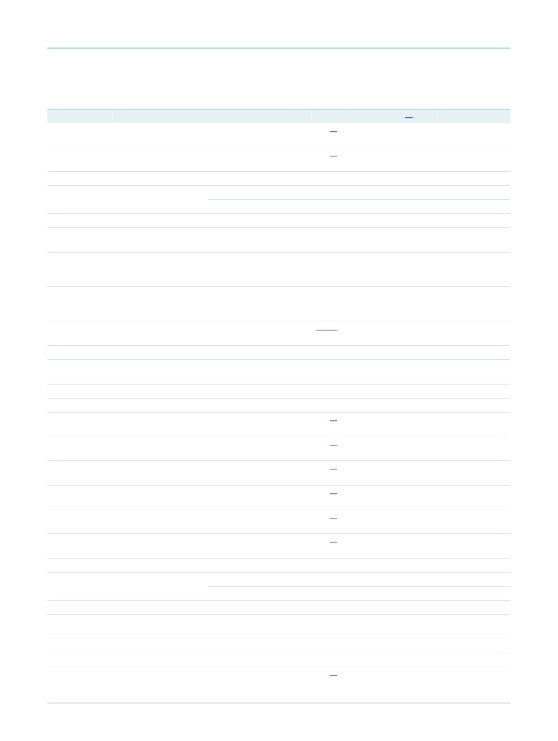
Table 7. Static characteristics …continued
T amb = ? 40 ° C to +85 ° C, unless otherwise specified.
LPC1111/12/13/14
Symbol
Parameter
Conditions
Min
Typ [1]
Max
Unit
I OHS
HIGH-level short-circuit V OH = 0 V
[6]
-
? 45
mA
output current
I OLS
LOW-level short-circuit
V OL = V DD(IO)
[6]
-
50
mA
output current
I pd
I pu
pull-down current
pull-up current
V I = 5 V
V I = 0 V
V DD(IO) < V I < 5 V
10
? 15
0
50
? 50
0
150
? 85
0
μ A
μ A
μ A
High-drive output pin (PIO0_7)
I IL
LOW-level input current V I = 0 V; on-chip pull-up
-
-
3
μ A
resistor disabled
I IH
HIGH-level input
V I = V DD(IO) ; on-chip
-
-
3
μ A
current
pull-down resistor
disabled
I OZ
OFF-state output
V O = 0 V; V O = V DD(IO) ;
-
-
3
μ A
current
on-chip pull-up/down
resistors disabled
V I
input voltage
pin configured to provide
[2][3][4]
-
5.0
V
a digital function
V O
V IH
output voltage
HIGH-level input
output active
0
2.0
-
-
V DD(IO)
-
V
V
voltage
V IL
V hys
LOW-level input voltage
hysteresis voltage
-
0.4
-
-
0.8
-
V
V
V OH
HIGH-level output
I OH = ? 4 mA
[5]
V DD(IO) ?
-
-
V
voltage
0.4
V OL
LOW-level output
I OL = 4 mA
[5]
-
0.4
V
voltage
I OH
HIGH-level output
V OH = V DD(IO) ? 0.4 V
[5]
20
-
-
mA
current
I OL
LOW-level output
V OL = 0.4 V
[5]
-
-
mA
current
I OHS
HIGH-level short-circuit V OH = 0 V
[6]
10
50
150
μ A
output current
I OLS
LOW-level short-circuit
V OL = V DD(IO)
[6]
? 15
? 50
? 85
μ A
output current
I pd
I pu
pull-down current
pull-up current
V I = 5 V
V I = 0 V
V DD(IO) < V I < 5 V
0
-
-
0
-
-
0
3
3
μ A
μ A
μ A
I 2 C-bus pins (PIO0_4 and PIO0_5)
V IH
HIGH-level input
0.7V DD(IO)
-
-
V
voltage
V IL
V hys
LOW-level input voltage
hysteresis voltage
-
-
-
0.5V DD(IO)
0.3V DD(IO)
-
V
V
V OL
LOW-level output
I OLS = 20 mA
[5]
-
0.4
V
voltage
LPC1111_12_13_14_0
? NXP B.V. 2009. All rights reserved.
Objective data sheet
Rev. 00.11 — 13 November 2009
31 of 53
发布紧急采购,3分钟左右您将得到回复。
相关PDF资料
MCB11C14
BOARD EVAL FOR NXP LPC11C14
MCB2470
BOARD EVAL NXP LPC247X SERIES
MCBSTM32EXL
BOARD EVALUATION FOR STM32F103ZE
MCBTMPM330
BOARD EVAL TOSHIBA TMPM330 SER
MCIMX25WPDKJ
KIT DEVELOPMENT WINCE IMX25
MCIMX53-START-R
KIT DEVELOPMENT I.MX53
MCM69C432TQ20
IC CAM 1MB 50MHZ 100LQFP
MCP1401T-E/OT
IC MOSFET DRVR INV 500MA SOT23-5
相关代理商/技术参数
MCB1114-ED
制造商:ARM Ltd 功能描述:KEIL NXP LPC1114 EVAL BOARD
MCB1114U
功能描述:开发板和工具包 - ARM EVAL BOARD FOR NXP LPC1114 + ULINK2
RoHS:否 制造商:Arduino 产品:Development Boards 工具用于评估:ATSAM3X8EA-AU 核心:ARM Cortex M3 接口类型:DAC, ICSP, JTAG, UART, USB 工作电源电压:3.3 V
MCB1114U-ED
制造商:ARM Ltd 功能描述:KEIL NXP LPC1114 EVAL BOARD
MCB1114UME
功能描述:开发板和工具包 - ARM EVAL BOARD FOR NXP LPC1114 + ULINK-ME
RoHS:否 制造商:Arduino 产品:Development Boards 工具用于评估:ATSAM3X8EA-AU 核心:ARM Cortex M3 接口类型:DAC, ICSP, JTAG, UART, USB 工作电源电压:3.3 V
MCB1114UME-ED
制造商:ARM Ltd 功能描述:KEIL NXP LPC1114 EVAL BOARD
MCB11C14
功能描述:开发板和工具包 - ARM EVAL BOARD FOR NXP LPC11C14
RoHS:否 制造商:Arduino 产品:Development Boards 工具用于评估:ATSAM3X8EA-AU 核心:ARM Cortex M3 接口类型:DAC, ICSP, JTAG, UART, USB 工作电源电压:3.3 V
MCB11C14-ED
制造商:ARM Ltd 功能描述:KEIL NXP LPC11C14 EVAL BOARD
MCB11C14U
功能描述:开发板和工具包 - ARM EVAL BOARD FOR NXP LPC11C14 + ULINK2
RoHS:否 制造商:Arduino 产品:Development Boards 工具用于评估:ATSAM3X8EA-AU 核心:ARM Cortex M3 接口类型:DAC, ICSP, JTAG, UART, USB 工作电源电压:3.3 V